Electronic Grade CVD
Overview
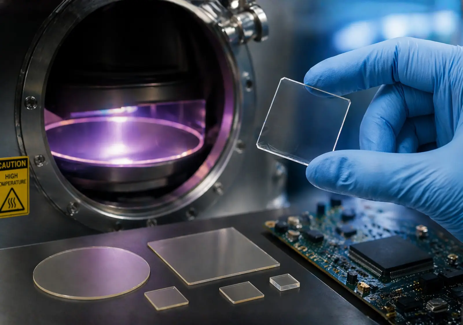
Advancements in chemical vapor deposition (CVD) technology have enabled the consistent production of high-purity diamonds engineered for advanced electronic and radiation detection applications. Electronic Grade CVD diamonds are developed as large-area, single-crystal plates and films through controlled homoepitaxial growth, ensuring exceptional material uniformity. These diamonds can be precisely tailored to meet the performance requirements of modern electronic systems, offering flexibility for a wide range of specialized applications.
Key Features
Available Variants
| Size | Thickness | Carat Weight |
|---|---|---|
| 2.0 × 2.0 mm | 0.50 mm | 0.03 ct |
| 3.0 × 3.0 mm | 0.50 mm | 0.08 ct |
| 4.5 × 4.5 mm | 0.50 mm | 0.17 ct |
| 2.0 × 2.0 mm | 0.30 mm | 0.02 ct |
| 3.0 × 3.0 mm | 0.30 mm | 0.05 ct |
| 4.5 × 4.5 mm | 0.30 mm | 0.10 ct |
Need a custom size or bulk order? Contact us for a quote.
Applications
RF Diodes
High-frequency signal processing and power conversion
BJT & FET
Bipolar Junction and Field Effect Transistors for advanced electronics
MEMS Devices
Micro-Electro-Mechanical Systems for sensors and actuators
Radiation Detection
Medical and industrial radiation monitoring applications
Radiotherapy Dosimetry
Precise radiation dose measurement for medical treatments
Power Electronics
High-power switching and conversion systems
Specifications
Ready to Get Started?
Contact our team to discuss your specific requirements and get a customized solution for your application.